How to fight back
Verification is eating the schedule
The 2024 Wilson Research Group Functional Verification Trend Reports point to a harsh reality: design complexity is rising faster than verification capacity, and the industry is paying for it in escapes, respins, and delays.
What the Wilson Research findings reveal
Two parallel stories show up loud and clear in the 2024 Wilson Research Group IC/ASIC Functional Verification Trend Report (further down “ASIC report”) and the 2024 Wilson Research Group FPGA Functional Verification Trend Report (further down “FPGA report”).
The uncomfortable truth: “done” doesn’t mean “correct”.
FPGA: bug escapes are the norm, not the exception
The FPGA report asks a direct question: how many non-trivial bugs escaped into production? The answer is sobering: in 2024, only 13% of FPGA projects reported zero non-trivial bug escapes—meaning 87% had at least one escape. (ref. the “Non-trivial bug escapes” discussion and Figure 3 on page 5 of the FPGA report).
The report also notes that, depending on the market (e.g., aerospace), fixing escapes can trigger revalidation and costly operational delays—not just a code change.
IC/ASIC: first-silicon success rate is at a two-decade low
The IC/ASIC report uses the classic effectiveness metric: how many spins before production? The headline result: in 2024, only 14% of IC/ASIC projects achieved first-silicon success, and the report calls this the lowest value recorded in the past 20 years (Figure 3 on page 5 of the ASIC report).
Different markets, different metrics—same message: teams are struggling to keep pace.
Schedules are slipping because verification work is expanding and is not predictable
Delays aren’t an edge case in chip design; they have become the baseline expectation. The ASIC report states that projects behind schedule increased to 75% in 2024 (page 6 of the ASIC report). The FPGA report shows that over two-thirds of FPGA projects were delayed. A little bit better, but still very far from good. (page 6, Figure 6 of the FPGA report).
And it’s not hard to see why: the almost continuous loop between verification and debugging is consuming the budget of time and people.
The villain: complexity growth across everything
Both reports point to similar complexity drivers—so this is not “just an FPGA problem” or “just an ASIC problem”.
SoC-class design is normal now
FPGA: 65% of FPGA projects target designs with one or more embedded processors; 43% include two or more. (Page 8 FPGA report)
IC/ASIC: 84% of projects incorporate embedded processors. (Page 8 ASIC report)
Once you add processors, you inherit whole new classes of verification challenges: HW/SW interaction, coherency, NoC-style interconnect, and system-level behavior.
Asynchronous clocks are everywhere
Both reports state that 95% of designs have two or more asynchronous clock domains (FPGA report page 8, ASIC report page 8). This drives verification workload because whole classes of metastability/CDC issues aren’t easily exposed by “just RTL sim.”
Security & safety are no longer “nice to have”
Security features: 62% of FPGA projects and 83% of IC/ASIC projects incorporate security features. (FPGA report page 9, ASIC report page 8.)
Safety-critical processes: 63% of FPGA projects adhere to one or more safety standards/guidelines; for IC/ASIC this is 44%. (FPGA report page 9, ASIC report page 9.)
Security and safety add requirements, scenarios, traceability, and compliance work—amplifying both verification volume and the cost of missing anything.
Verification maturity is rising… but the bottleneck isn’t gone
Both reports highlight increasing adoption of more mature verification practice patterns:
Accelera UVM is the leading standard for creating FPGA testbenches (close to 50%, page 10 of the FPGA report). Other methodologies have also been gaining traction in FPGA, such as the Open Source VHDL Verification Methodology™ (OSVVM) in ~35% and the Universal VHDL Verification Methodology (UVVM) in ~28%. In IC/ASIC, UVM comes even close to 80% adoption.
Formal verification techniques are also climbing—helped by “automatic” applications that reduce the expertise barrier. FPGA formal adoption is increasing at ~7.5% CAGR (FPGA report page 11) and IC/ASIC formal property checking adoption increases by ~5.8% CAGR, and automatic formal applications by ~8.7% CAGR (ASIC report page 11).
Nevertheless, the FPGA non-trivial bug escape rate continues to grow, and the first-silicon success rate in ASIC is at an all-time low.
Debug eats the calendar (and management can’t estimate it)
Both reports say the same thing in slightly different wording: verification engineers spend more time debugging than on any other task, and that creates a planning nightmare.
With 47% of their time spent on debugging (reports page 7), it is the largest slice of FPGA and ASIC verification engineer time. From a management perspective, this poses a considerable challenge when planning future projects, as debugging is highly unpredictable and can vary significantly between projects, making it difficult to rely on previous project data for accurate effort and scheduling estimates.
The impact is enormous. Not only because of the risks and the waste of time and money, but also planning becomes a nightmare. Debugging varies significantly between projects, which explains why planning the effort and schedule for new projects based on previous ones is so difficult from a management perspective—and why so many projects end up behind schedule.
Sigasi, your first line of defense
So where do you attack the problem? You don’t “solve” debugging—but you can reduce the amount of errors to be debugged. “Easy errors” that shouldn’t exist in the first place.
Shift-left: kill trivial (and many non-trivial) bugs before simulation starts
Sigasi Visual HDL helps teams shift-left by catching issues while design engineers are writing code, reusing IP or even integrating AI generated code. Through a patented superfast real-time language model that acts like an always-on compiler, engineers get immediate feedback inside VS Code instead of discovering errors late—during integration, simulation bring-up, or (worst) in the lab.
What that changes in practice:
- You catch easy-to-fix defects early, when context is fresh in the design engineer’s mind and changes are cheap.
- You reduce “noise” in the verification pipeline, so verification engineers can focus on hard bugs and corner cases.
- You reduce the chance that avoidable issues turn into late-stage schedule slips or escapes that leak into silicon or production.
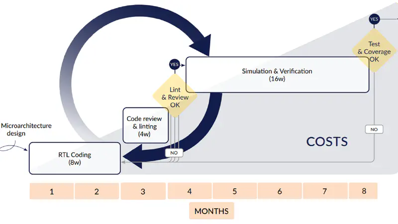
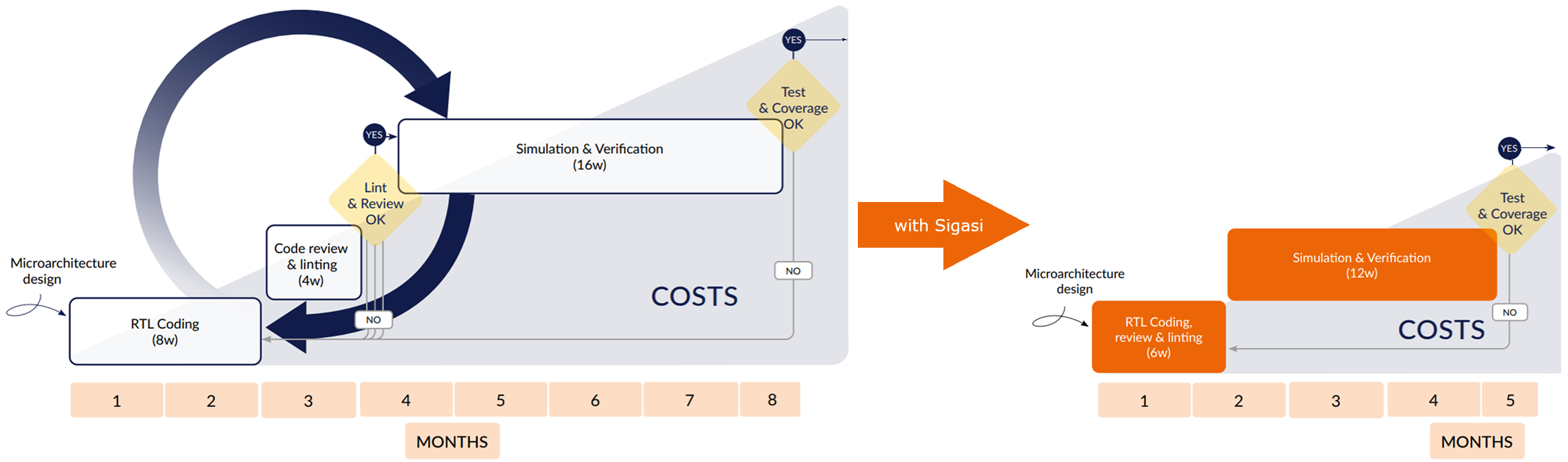
If your verification (and design) engineers have better things to do than spending most of their time chasing trivial bugs, it’s time for Sigasi. The result is clear. On average our customer report a reduction from 30 weeks to 20 weeks. That’s 33% less!
Lets smash those bugs together
Our support engineers — hands-on, with extensive FPGA and ASIC design and verification experience — are happy to show how “shift-left” is done in our Sigasi Verification Frameworks webinar which is available on demand as it was broadcasted on on Wednesday, 28th of January. Watch it now.
2025-12-12, last modified on 2026-02-11